Volume 2-0617

June 2017
order form
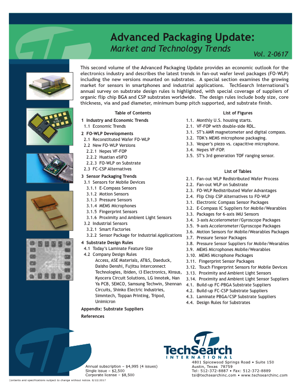
The Advanced Packaging Update (2-0617) provides an economic outlook for the electronics industry and describes the latest trends in fan-out wafer level packages (FO-WLP) including the new versions mounted on substrates. A special section examines the growing market for sensors. TechSearch International’s annual survey on substrate design rules is highlighted, with special coverage of suppliers of organic flip chip BGA and CSP substrates worldwide. The design rules include body size, core thickness, via and pad diameter, minimum bump pitch supported, and substrate finish.
  • Contents…
    • 1 Industry and Economic Trends
      • 1.1 Economic Trends
        • 1.1.1 U.S. Macroeconomic Trends
    • ​2 FO-WLP Developments
      • 2.1 Reconstituted Wafer FO-WLP​
      • 2.2 New FO-WLP Versions
        • 2.2.1 Nepes VF-FOP
        • 2.2.2 Huatian eSiFO
        • 2.2.3 FO-WLP on Substrate
      • 2.3 FC-CSP Alternatives
    • 3 Sensor Packaging Trends
      • 3.1 Sensors for Mobile Devices
        • 3.1.1 E-Compass Sensors
        • 3.1.2 Motion Sensors
        • 3.1.3 Pressure Sensors
        • 3.1.4 MEMS Microphones
        • 3.1.5 Fingerprint Sensors
        • 3.1.6 Proximity and Ambient Light Sensors
      • 3.2 Industrial Sensors
        • 3.2.1 Smart Factories
        • 3.2.2 Sensor Package for Industrial Applications
    • 4 Substrate Design Rules
      • 4.1 Today's Laminate Feature Size
      • 4.2 Company Design Rules
        • 4.2.1 Access
        • 4.2.2 ASE Materials
        • 4.2.3 AT&S
        • 4.2.4 Daeduck
        • 4.2.5 Daisho Denshi Co., Ltd.
        • 4.2.6 Fujitsu Interconnect Technologies, Ltd.
        • 4.2.7 Ibiden Co., Ltd.
        • 4.2.8 i3 Electronics
        • 4.2.9 Kinsus Interconnect Technology Corp.
        • 4.2.10 Kyocera Circuit Solutions
        • 4.2.11 LG Innotek
        • 4.2.12 Nan Ya PCB Corporation
        • 4.2.13 Samsung Electro-Mechanics Ltd.
        • 4.2.14 Samsung Techwin
        • 4.2.15 Shennan Circuits, Co., Ltd.
        • 4.2.16 Shinko Electric Industries Co., Ltd.
        • 4.2.17 Simmtech Co., Ltd.
        • 4.2.18 Toppan Printing Co., Ltd.
        • 4.2.19 Tripod Technology Corporation
        • 4.2.20 Unimicron Technology Corporation
    • Appendix: Substrate Suppliers
    • References
  • Figures…
    • 1.1 Monthly U.S. housing starts.
    • 2.1 VF-FOP with double-sided RDL.
    • 3.1 ST's AMR magnetometer and digital compass.
    • 3.2 TDK's second-generation MEMS microphone packaging.
    • 3.3 Vesper's piezoelectric microphone versus capacitive type.
    • 3.4 Nepes VF-FOP.
    • 3.5 ST's third-generation TOF ranging sensor with integrated lenses.
  • Tables…
    • 2.1 Fan-out WLP Redistributed Wafer Process Types
    • 2.2 Fan-out WLP on Substrate
    • 2.3 FO-WLP Redistributed Wafer Advantages
    • 2.4 Flip Chip CSP Alternatives to FO-WLP
    • 3.1 Electronic Compass Sensor Packages
    • 3.2 Suppliers of E-Compass ICs for Mobile and Wearable
    • 3.3 Packages for 6-axis IMU Sensors
    • 3.4 Packages for 3-axis Accelerometers and Gyroscopes
    • 3.5 Packages for 9-axis Accelerometers and Gyroscopes
    • 3.6 Suppliers of Motion Sensors for Mobile and Wearables
    • 3.7 Pressure Sensor Packages
    • 3.8 Suppliers of Pressure Sensors for Mobile and Wearables
    • 3.9 Suppliers of MEMS Microphones for Mobile and Wearables
    • 3.10 MEMS Microphone Packages
    • 3.11 Fingerprint Sensor Packages
    • 3.12 Touch Fingerprint Sensors for Mobile Devices
    • 3.13 Proximity and Ambient Light Sensors Packages
    • 3.14 Proximity and Ambient Light Sensor Suppliers
    • 4.1 Selected Build-up FC-PBGA Substrate Suppliers
    • 4.2 Selected Build-up FC-CSP Substrate Suppliers
    • 4.3 Selected Laminate PBGA/CSP Substrate Suppliers
    • 4.4 Design Rules for ASE PBGA/CSP Substrates
    • 4.5 Design Rules for AT&S FC-PBGA Substrates
    • 4.6 Design Rules for Daeduck FC-CSP Substrates
    • 4.7 Design Rules for Daeduck Thin Build-Up WB Substrates
    • 4.8 Design Rules for Daisho Denshi PBGA/CSP Substrates
    • 4.9 Design Rules for FICT FC-PBGA Substrates
    • 4.10 Design Rules for Ibiden FC-PBGA Substrates
    • 4.11 Design Rules for Ibiden FC-CSP Substrate
    • 4.12 Design Rules for Ibiden Coreless Substrates
    • 4.13 Design Rules for CoreEZ® Substrates
    • 4.14 Design Rules for HyperBGA® Substrate
    • 4.15 Design Rules for i3 Electronics PBGA Substrates
    • 4.16 Design Rules for MicroFlex (Polyimide)
    • 4.17 Design Rules for Kinsus FC-PBGA Substrates
    • 4.18 Design Rules for Kinsus FC-CSP Substrates
    • 4.19 Design Rules for Kinsus PBGA/CSP Substrates
    • 4.20 Design Rules for Coreless Substrates
    • 4.21 Design Rules for Kyocera FC-PBGA Substrates
    • 4.22 Design Rules for Kyocera FC-CSP Substrates
    • 4.23 Design Rules for Kyocera Coreless Substrates
    • 4.24 Design Rules for LG Innotek CSP Substrates
    • 4.25 Design Rules for LG Innotek FC-CSP Substrates
    • 4.26 Design Rules for Nan Ya PCB FC-PBGA Substrates
    • 4.27 Design Rules for Nan Ya PCB PBGA/CSP Substrates
    • 4.28 Design Rules for Nan Ya FC-CSP Substrates
    • 4.29 Design Rules for Nan Ya PCB FC-PBGA Coreless Substrates
    • 4.30 Design Rules for SEMCO FC-PBGA Substrates
    • 4.31 Design Rules for SEMCO PBGA/CSP Substrates
    • 4.32 Design Rules for SEMCO FC-CSP Substrates
    • 4.33 Design Rules for SCC PBGA/CSP Substrates
    • 4.34 Design Rules for Shinko Electric FC-PBGA Substrates
    • 4.35 Design Rules for Shinko Electric FC-CSP Substrates
    • 4.36 Design Rules for Shinko Electric Coreless Substrates
    • 4.37 Design Rules for Shinko Electric PBGA/CSP Substrates
    • 4.38 Design Rules for Simmtech PBGA/CSP Substrates
    • 4.39 Design Rules for Simmtech Coreless Substrates
    • 4.40 Design Rules for Toppan FC-PBGA Substrates
    • 4.41 Design Rules for Coreless Substrates
    • 4.42 Design Rules for Tripod PBGA/CSP Substrates
    • 4.43 Design Rules for Unimicron FC-PBGA Substrates
    • 4.44 Design Rules for Unimicron FC-CSP Substrates
    • 4.45 Design Rules for Unimicron PBGA/CSP Substrates
Stacks Image 25201
brochure
  • Published June 2017
  • 80 pages
  • 7 figures / 63 tables
  • 45 PowerPoint slides
  • $4,995 annual subscription (4 issues)
    $2,500 single issue
    $8,500 corporate license
Who We Are
TechSearch International is recognized around the world as a leading consulting company in the field of advanced semiconductor packaging and assembly, electronics manufacturing, and materials.
Network
Contact
  • email message
  • +1.512.372.8887
  • +1.512.372.8889
  • 4801 Spicewood Springs Rd, Ste 150
    Austin, TX 78759
    United States