
Trusted source for semiconductor packaging analysis since 1987
2025 Flip Chip and WLP
Trends and Market Forecasts
-
Deep analysis of drivers for fan-in WLP, FO-WLP, panel FO, and flip chip demand with future market projections
-
Technology developments in wafers and panel processing, WLP reliability, flip chip bumps and substrates, underfills, hybrid bonding, and more
-
Examinations of packages, die, bump, and RDL characteristics from recent TechSearch International teardowns
-
Wafer demand vs. capacity for flip chip and WLP

APU Vol. 3-1125
Advanced Packaging Update

-
Introduction
We are recognized around the world as a leading consulting company in the field of advanced semiconductor packaging technology.
Our goal is to enable our clients to compete more effectively by providing accurate, relevant, and timely information on technology trends and market developments.
We provide strategic market analysis, competitive analysis, technology trends, and evaluation of product strategies in the areas of semiconductor packaging and assembly, electronics manufacturing, and materials.
What sets TechSearch apart from others?- We have close relationships with companies and industry leaders built on trust and mutual respect
- We ask customers what they want—report content is constantly tailored to meet those needs
- We provide complete, concise, accurate data and unbiased opinions
- We participate in many industry conferences to share our findings and stay up-to-date on the latest innovations
- We frequently tour PCB, EMS, and OSAT manufacturing facilities
-
Advanced Packaging Update
The Advanced Packaging Update (4 issues per year) features special coverage of market and technology developments for BGAs, CSPs, stacked die CSPs, flip chip, and wafer level packages. Each issue includes new applications, developments in materials and assembly equipment, and new package constructions.
Topics covered include:- Stacked die CSP trends
- Packaging trends for mobile products such as smartphones including color photos and x-rays of components
- System-in-package (SiP), multichip modules, and multichip packages
- Interposer developments including silicon, organic, and glass
- Reliability test results for new packages
- New assembly materials
- Substrate design rules and trends
- New wafer level package versions and suppliers
- Embedded component packages
- Power device packages
- DRAM packaging trends
- Assembly issues for silicon with low-k dielectrics
- Developments in Pb-free packaging
-
Multi-client Analysis
-
Single-client Consulting
-
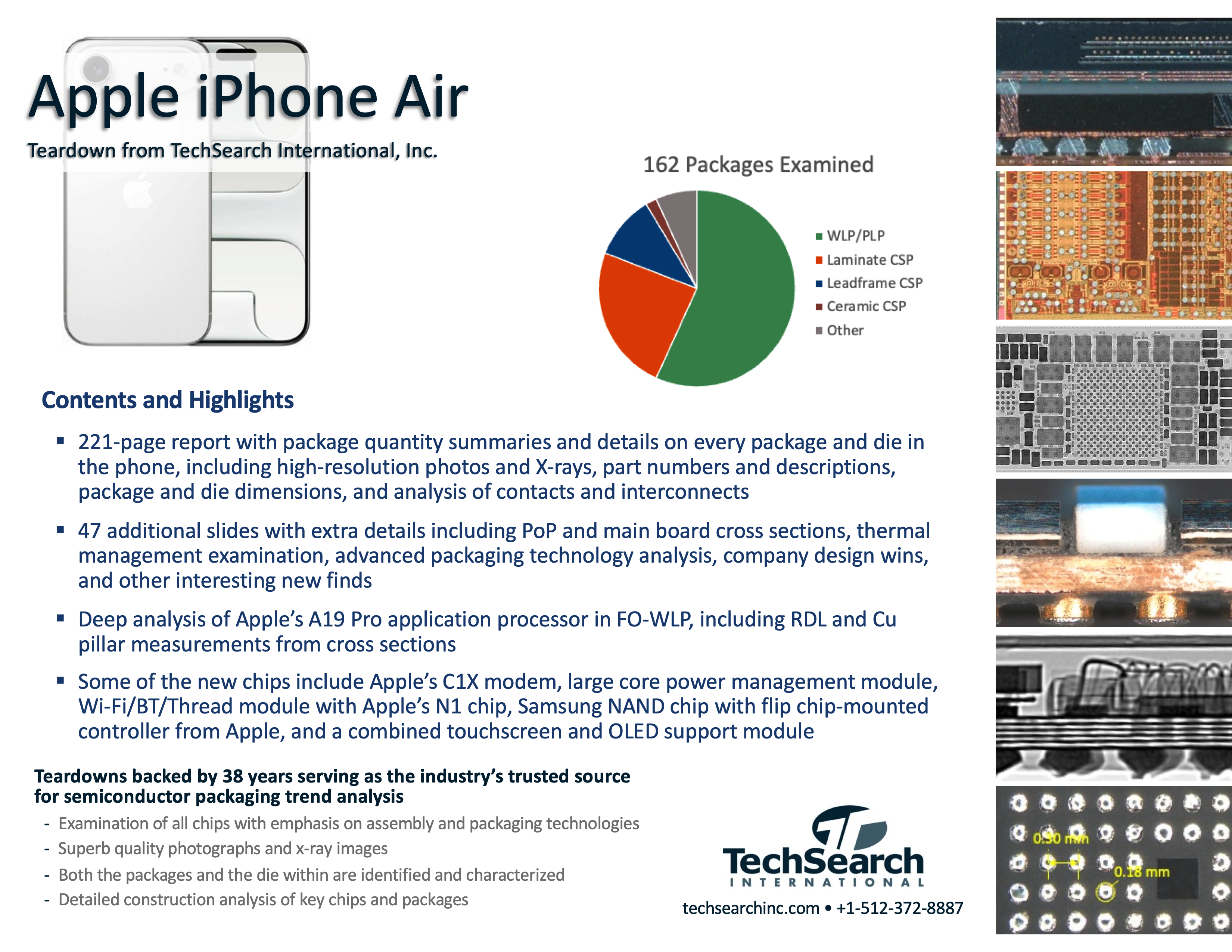
Teardowns of System Products and Packages
TechSearch International's deep understanding of advanced packaging technologies is supported by teardowns of leading-edge system products. We perform our own teardowns and utilize third-party services of other experts. Information from the teardowns can be found throughout our line of reports. We also provide to clients individual teardown reports.
-
IPC Study - Analysis of Semiconductor and Advanced Packaging Ecosystem
TechSearch International president Jan Vardaman served as co-author on a study from IPC that provides a thorough, data-driven analysis of the global semiconductor and advanced packaging ecosystem. The study, An Analysis of the North American Semiconductor and Advanced Packaging Ecosystem, highlights the role of advanced packaging in driving innovation in semiconductor designs.
-
Worldwide Assembly & Test Facility Database
In partnership with SEMI®, we offer a comprehensive data file tracking over 500 total back-end facilities of IDMs and outsourced semiconductor assembly and testing manufacturers. This database offers access to and insights into global OSAT facilities in China, Taiwan, Korea, Japan, Southeast Asia, Europe, and the Americas. The report also highlights packaging technology offerings by manufacturing location
-
Global Semiconductor Packaging Materials Outlook
In partnership with TECHCET and SEMI®, we offer a comprehensive market research study that examines semiconductor packaging trends and their impact on the packaging materials markets. Markets are quantified, new opportunities are highlighted for advanced technology nodes and emerging package form factors, and the materials market outlook is presented.
-
Packaging Cost Models—Fan-out WLP, WLP, flip chip, and more
In partnership with SavanSys Solutions, TechSearch International provides access to valuable cost models for packaging. SavanSys develops the models and we help to calibrate the data. Available are cost models for fan-out wafer level packaging, WLP, 2.5D and 3D packaging, flip chip, and wire bond applications.

IEEE Frances B. Hugle Engineering Scholarship, established by IEEE and TechSearch International
In celebration of TechSearch International’s 25th anniversary, we partnered with IEEE Women in Engineering Committee (WIE) to establish a scholarship for women going into the field of engineering.
The scholarship, named the IEEE Frances B. Hugle Engineering Scholarship, honors the memory of the distinguished engineer for whom the fund is named. Frances Hugle graduated from the University of Chicago in 1946 with degrees in chemistry, physics, and philosophy and received her M.Sc. degree from the University of Cincinnati. She co-founded Hugle Industries, Siliconix, Stewart Warner Microcircuits, Inc. and Opto-Electronics Devices, Inc. In each of these companies she served as a director of R&D and as chief engineer. She held 16 known patents in the field of electronics and was one of the pioneers in the invention of tape automated bonding (TAB).
To encourage young women to follow in Hugle’s footsteps, IEEE WIE selects one scholar annually to receive a $2,500 scholarship. The scholarship is presented to one female in her third year of undergraduate study in an engineering curriculum at an accredited university or college in the United States. Student membership in the IEEE is required. To apply, visit wie.ieee.org/francesbhugle.
Our company started the contributions with a donation of $5,000 in December 2012 and we have continued the scholarship program ever since. We hope that your company will join us by making a contribution.
The IEEE Foundation, a tax exempt 501(c)(3) organization in the United States, is accepting and managing the donations. Donations can be made by:
1. Online at ieee.org/donate by selecting the Frances B. Hugle Memorial Fund
2. By check payable to the IEEE Foundation – Frances B. Hugle Memorial Fund and mailed to IEEE Foundation, 445 Hoes Lane, Piscataway, NJ, 08854, USA.
Donations are tax deductible to the fullest extent allowed by law in the United States. For other countries, please check with your local tax advisor. All donations of $25 or more receive an acknowledgement letter for tax purposes. To learn more about the IEEE Foundation, visit ieeefoundation.org or call the IEEE Development Office at +1 732-562-3915 or email donate@ieee.org. For more information on IEEE WIE, visit ieee.org/women. For more information about the scholarship, visit wie.ieee.org/francesbhugle.
Thank you for helping to encourage young females to pursue their passions and explore their inventive spirit.
- email message
- +1.512.372.8887
- +1.512.372.8889
- 4801 Spicewood Springs Rd, Ste 150
Austin, TX 78759
United States


